STM32H747 Memory Architecture Navigating the Bus Matrix in an Audio + TouchGFX Project
Engineering notes from a Music Player project, built on the STM32H747I-DISCO, where memory placement decisions were the difference between a working system and a frozen LCD.
For embedded software and hardware engineers working with STMicroelectronics MCUs — particularly anyone moving from an STM32F4 / L4 to the high end H7 family for the first time, or anyone debugging unexplained DMA, cache, or LCD-tearing bugs on a dual-core H7.
1. Introduction — Why STM32H747 Memory Architecture Matters
At a glance
The STM32H747 is a high-end dual-core Cortex-M7 + Cortex-M4 MCU with three independent power domains, eight SRAM regions, four DMA controllers, and a multi-master bus matrix. Default linker placement works for trivial projects and quietly breaks for everything more complex — audio capture stutters, LCD framebuffers tear, UART RX silently drops bytes. This post documents the architectural rules that prevent those failure modes, with worked examples from a real product: a Music Player by Voice Command, built end-to-end on the STM32H747I-DISCO with TouchGFX on the LCD, FreeRTOS coordinating audio capture, SD persistence, UART streaming to a Wi-Fi companion, and cloud Speech-to-Text. The cloud connection itself was handled by a u-blox NORA-W106-00B Wi-Fi/Bluetooth module (ESP32-S3 inside, no PSRAM on this variant) acting as the STM32’s Wi-Fi front-end; the NORA receives audio over UART from the STM32, opens a TLS session, and uploads to Google Cloud Storage + Speech-to-Text. If you read only one section, read [Section 8: Hard Rules — Where Each Buffer Class Belongs](#8-hard-rules-where-each-buffer-class-belongs-on-stm32h7).
Motivation — the problem this post solves
If you’ve ever built anything beyond a hello-blink on an STM32H7, you’ve probably hit at least one of these:
- A FreeRTOS queue that worked yesterday breaks today after an unrelated refactor — and no code in your queue path changed.
- LCD tearing or FUIF (FIFO underrun) interrupts firing during heavy CPU work, with no obvious culprit.
- DMA transfers that “complete successfully” but the CPU reads stale data, or transmits stale data.
- Audio capture works on the bench but glitches every few seconds when the LCD redraws.
- Random HardFaults that disappear when you add a printf for debugging.
Every one of these is a memory architecture symptom. None of them are bugs you can find by reading the code line by line. They’re bugs that come from the H7’s distributed memory map being treated as a flat SRAM blob, which is the model embedded engineers carry over from simpler MCUs. The H7 doesn’t work that way, and the silicon won’t tell you when you’ve placed a buffer in a region that doesn’t suit it — the compiler is silent, the linker is silent, and at runtime the bug shows up as non-deterministic glitches.
This post is a practical walkthrough of how to think about H7 memory placement before those symptoms appear, written from the trenches of a real product. Everything here was learned the hard way; everything is traceable to a .map file, a register dump, or an RTT log. That said, the fact that we used excellent tools from IAR Embedde Workbench ( cspybat, C-SPY macros) and SEGGER (J-Link, RTT, RTT Viewer, J-Link Commander) made it dramatically simpler to debug each issue and pinpoint exactly where the fault was — without those tools, the same investigation would have taken days instead of hours.
A high-level overview of the STM32H747
The STM32H747 is at the top end of STMicroelectronics’s general-purpose Cortex-M lineup. The key specs that drive everything in this post:
- Dual-core architecture. A Cortex-M7 main core running up to 480 MHz (400 MHz in our build for thermal headroom), plus a Cortex-M4 co-processor running up to 240 MHz. The two cores share Flash and most peripherals but each has its own L1 cache, its own NVIC, and its own bus-master ports into the system bus matrix. On this project we use the M7 exclusively; the M4 holds a stop-mode stub for future low-power offload.
- Three independent power domains (D1, D2, D3). Each domain has its own clock gate, voltage regulator, and SRAM. Domains can be powered down independently, which enables low-power modes where only D3 stays alive listening for wake events.
- 1 056 KB of internal SRAM total, split across at least five distinct regions — D1 AXI SRAM (512 KB), D2 SRAM1/2/3 (128 + 128 + 32 = 288 KB combined), D3 SRAM4 (64 KB), plus D1 DTCM (128 KB) and ITCM (64 KB) tightly coupled to the M7. There is also a 4 KB battery-backed SRAM in the D3 backup region for state that survives across power loss.
- 2 MB Flash, dual-bank, with read-while-write support for in-field firmware updates.
- Four DMA controllers with different domain reach: MDMA (cross-domain), DMA1/DMA2 (D2-rooted, can reach D1+D2), BDMA (D3-only). Plus DMA2D for graphics blitting and dedicated IDMAs inside SDMMC and JPEG.
- A rich peripheral set: dual Ethernet MAC, USB OTG HS/FS, multiple SAI (audio), DFSDM (digital filter for sigma-delta — what we use for PDM mic capture), FMC (external memory controller), QUADSPI, LTDC (LCD-TFT controller) with up to 24-bit RGB output, DSI host for MIPI-DSI panels, hardware JPEG codec, DMA2D 2D blitter, two SDMMC controllers, and the usual array of UARTs, SPIs, I2Cs, timers and ADCs.
- High-end Cortex-M7 features: 16 KB + 16 KB L1 caches (instruction + data), single-precision + double-precision FPU, MPU with 16 regions, and full CoreSight trace (ETM, ITM, DWT) brought out to SWO and trace pins.
What ST built this for
The H7 is targeted at applications that need MCU-level real-time determinism and near-MPU-level compute. The canonical use cases are: graphical user interfaces driving large colour TFT panels (TouchGFX, Embedded Wizard, LVGL, Crank ); industrial control with simultaneous Ethernet + CAN + motor-control PWM; high-resolution audio capture, processing and streaming (PDM mic arrays, multi-channel SAI, USB Audio Class); medical and instrumentation devices that combine signal acquisition, on-device DSP, and a touch screen; and any product where a single chip needs to drive a display, talk to a cloud, and run sensor pipelines simultaneously. This project — voice capture, cloud STT, and a TouchGFX UI on one chip — is squarely in that envelope.
The specific project this post is built from
This post is a retrospective on the memory-architecture work for a voice-controlled music player built on the STM32H747I-DISCO development board. The STM32 records audio from the onboard MP34DT05-A PDM microphone using DFSDM in Sinc3 mode at 16 kHz, persists the WAV file to SD card via SDMMC, and streams it over UART8 to a Wi-Fi companion module that handles the cloud upload and speech-to-text call. The companion module is treated as an opaque endpoint in this post — every technical detail below concerns the STM32 side: how the audio buffers are placed, how the DMA paths are routed, how the FreeRTOS objects are pinned, and how the LCD framebuffer coexists with the audio path on the bus matrix. In parallel with audio, a TouchGFX UI renders to the 800×480 RGB DSI panel using a partial-framebuffer (PFB) strategy. FreeRTOS coordinates seven concurrent tasks on the M7: voice recording, SD-card writing, UART RX, command handling, RTT logging, TouchGFX rendering, and a low-priority video-frame task.
The toolchain used throughout this post: IAR Embedded Workbench 9.70.2 for compile + link, `cspybat` (IAR’s command-line C-SPY runner) for headless automated debug probes, C-SPY macros (.mac files) for scripted breakpoint actions, SEGGER J-Link as the SWD probe, SEGGER RTT for zero-overhead real-time logging, SEGGER J-Link RTT Viewer (the standalone GUI host tool) for watching RTT channels live during development, JLinkRTTLogger for capturing RTT channels to file unattended, and J-Link Commander for free-running register/memory inspection while the target runs. The combination of these tools is what made it feasible to diagnose the memory-related bugs described later in the post without ever using printf.
What you’ll learn from this post
The H7’s three-domain layout and the engineering reasons ST chose it. The fixed peripheral memory map and which DMA controllers can reach which peripherals. How the AHB bus matrix and MDMA tie the domains together. A concrete block diagram of one real project’s tasks and buffers. How to read a linker .map file to verify placement decisions. The three classes of memory collision (spatial, bus contention, cache coherency) and how to fix each. A practical workflow for debugging real-time systems with zero CPU overhead using SEGGER RTT, cspybat, and C-SPY macros. A short rule book I now apply to every H7 project.
Every example below is from real firmware on this project and every decision is traceable back to a .map file or a .icf linker script committed to the project repository.
2. STM32H747 Memory Domain Overview
STM32H7 memory architecture diagram showing the three power domains D1 D2 D3 with their SRAMs and DMA controllers](images/stm32h7-memory-architecture-domains.png “STM32H7 memory architecture — three-domain layout (D1 core, D2 peripheral, D3 low-power)”)
The H747 silicon is partitioned into three power domains. Each owns its own clock gate, voltage regulator, can sleep independently, and contains its own SRAM and peripherals.
Table 2.1 — STM32H7 power domains side-by-side
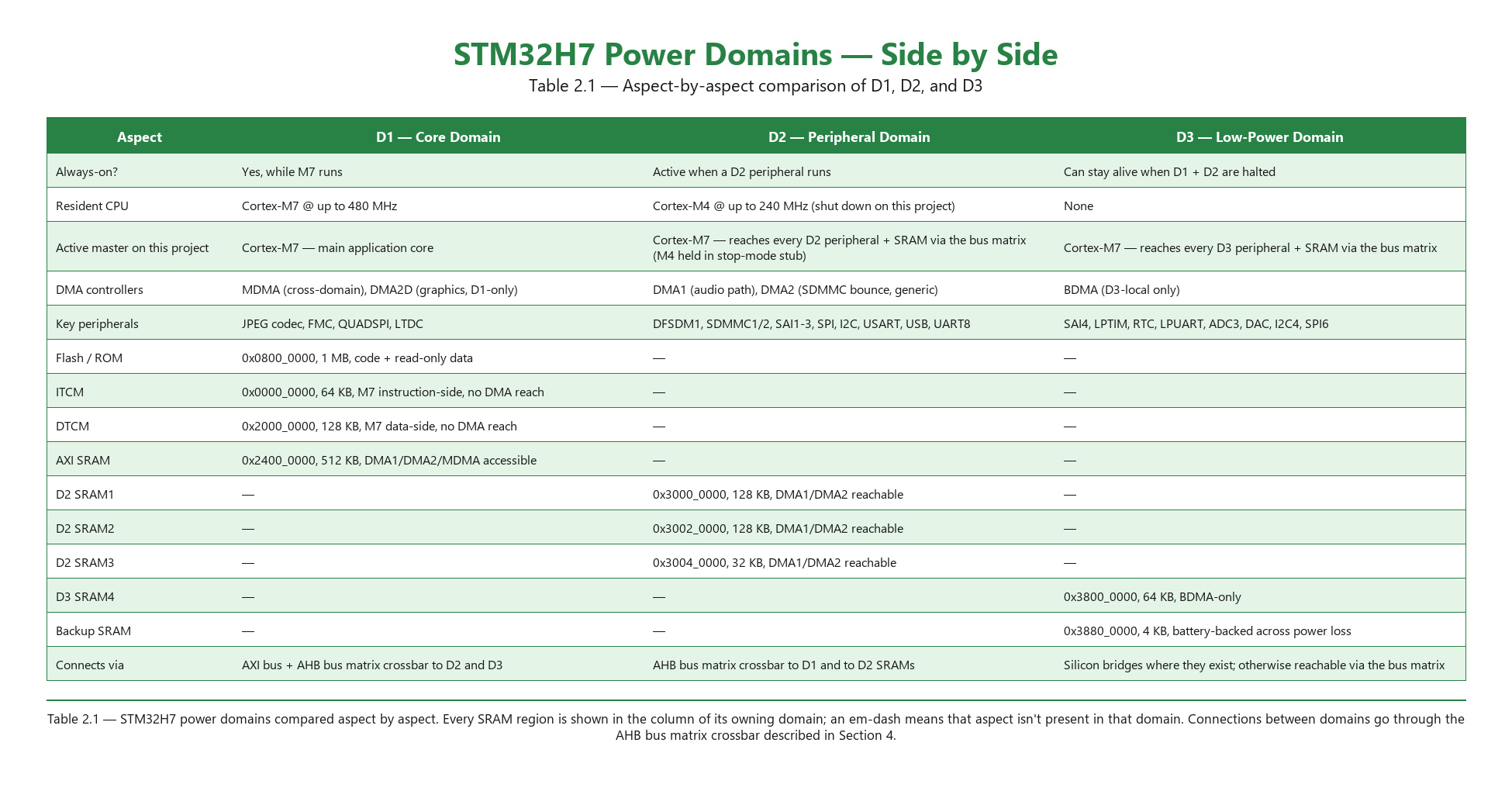
The names get easier once you stop reading “D1, D2, D3” as ordinal and start reading them as purpose: D1 is for processing, D2 is for peripherals, D3 is for whatever has to stay alive when most of the chip is asleep. Everything else falls out of that.
3. STM32H747 Peripheral Memory Map — Where Each Peripheral Lives
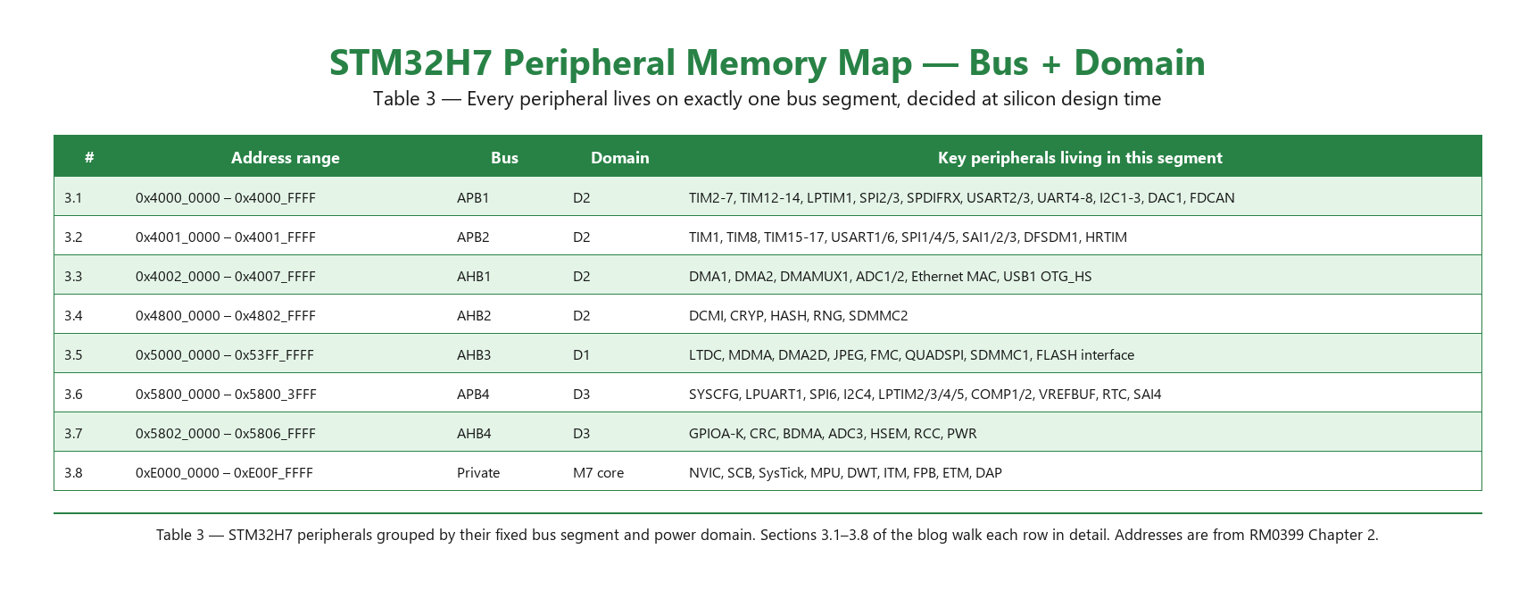
Beyond the SRAM regions, every peripheral on the H747 lives at a fixed memory address. These addresses are baked into the silicon and never change; they’re how the CPU and DMA controllers reach each peripheral’s registers. Knowing this map matters for three concrete reasons: (a) choosing the right DMA controller, because each peripheral has fixed DMA request lines that pair with specific DMA streams; (b) debugging via direct memory access, because a J-Link command like mem32 0x40017000 reads DFSDM1 channel 0’s CHCFGR1 register regardless of whether any debug symbols are loaded; and (c) understanding why peripherals in the same domain share clock-gate behaviour and power-mode reach.
The table below summarises the major peripheral bus segments on the STM32H747. Each row maps an address range to its bus (APB1–4 or AHB1–4), its power domain (D1, D2, or D3), and the key peripherals living there. Numbered descriptions in sections 3.1–3.8 below explain each row in detail.
A quick refresher — AHB vs APB
Before diving into each row, it helps to remember what “AHB” and “APB” actually mean, because the names appear in every row of the table above and the difference is the reason peripherals are split across them in the first place.
Both AHB and APB are bus protocols defined by the AMBA specification that ARM publishes for its Cortex cores. They were designed in tandem to serve two different bandwidth/cost trade-offs in a single chip:
- AHB — Advanced High-performance Bus. Full clock-rate (in the H7, 200 MHz HCLK). Supports multiple bus masters with hardware arbitration, burst transfers, pipelined transactions, and wide 32-bit data paths. Designed for the throughput-heavy traffic of DMA controllers, the LCD controller, the Ethernet MAC, the SDMMC controllers, the memory controllers (FMC, QUADSPI), and the graphics blitter (DMA2D). Anything that needs to move bytes by the thousands per millisecond lives on an AHB segment.
- APB — Advanced Peripheral Bus. Half clock-rate (in the H7, 100 MHz = HCLK/2). Single-master (the CPU’s AHB-to-APB bridge), no bursts, simpler handshake, lower gate count, lower power. Designed for the slower-but-numerous register-mapped peripherals — UARTs, I2Cs, SPIs, timers, DAC, comparators, the RTC, basic SAI. The CPU writes a register, the peripheral acts on it, the peripheral generates a slow IO signal. None of that needs 200 MHz throughput.
On the H7, the bus matrix exposes AHB1–AHB4 as the high-speed segments and APB1–APB4 as the low-speed segments — one of each per power domain (roughly), plus the D1-specific AHB3 that hosts the heaviest D1 masters. Knowing which segment a peripheral lives on tells you (a) its register-access clock rate, (b) whether DMA can fan in from multiple sources at once, and (c) what the upper bound on its sustained data rate is. The rest of this section walks each segment in detail.
3.1 APB1 — D2 peripheral domain, slower bus
APB1 is the lower-speed peripheral bus, running at HCLK/2 (typically 100 MHz when the M7 is at 400 MHz). It hosts the bulk of general-purpose communication peripherals: the lower-numbered timers (TIM2-7 and TIM12-14), most UARTs (UART4-8, USART2/3), all I2C controllers, most SPI controllers, the DAC, FDCAN, and SPDIFRX. UART8 on this project — the link to the Wi-Fi companion module — is mapped at 0x4000_7C00. APB1’s relatively low clock means most APB1 peripherals can be driven at line rate without contention even when D1 is heavily loaded.
3.2 APB2 — D2 peripheral domain, faster bus
APB2 also runs at HCLK/2 (100 MHz max in the typical configuration), but its peripherals are the higher-bandwidth ones: the advanced timers (TIM1, TIM8, TIM15-17, HRTIM), the fast SPI/SAI controllers, USART1/6, and crucially DFSDM1, which drives the PDM microphone capture on this project. DFSDM1 sits at 0x4001_7000. Its DMA pairings route to DMA1/DMA2 channels through DMAMUX1; both of those DMA controllers live in the same D2 domain, which is why DFSDM-to-RAM transfers don’t need to cross the bus matrix to reach D2 SRAM1.
3.3 AHB1 — D2 peripheral domain, DMA + high-speed peripherals
AHB1 is the high-speed peripheral bus, running at HCLK directly (200 MHz). It hosts the DMA controllers (DMA1, DMA2) and their request multiplexer (DMAMUX1), along with the Ethernet MAC, USB1 OTG_HS, and the first two ADCs. The DMA controllers’ register banks sit at 0x4002_0000 (DMA1) and 0x4002_0400 (DMA2). When firmware writes to a DMA stream’s configuration registers (CR, NDTR, M0AR, etc.), it’s writing here — the actual data movement happens through the AHB-master ports of the DMA blocks, not through these register accesses.
3.4 AHB2 — D2 peripheral domain, security + camera + SD
AHB2 hosts the security/crypto block (CRYP, HASH, RNG), the digital camera interface (DCMI), and the second SD/MMC controller (SDMMC2). SDMMC2 is functionally identical to SDMMC1 (which is on AHB3 in D1) — the difference is which domain’s DMA can reach it most cheaply. SDMMC2 in D2 pairs naturally with DMA1/2 in D2; SDMMC1 in D1 pairs naturally with MDMA.
3.5 AHB3 — D1 core domain, graphics + JPEG + memory controllers
AHB3 is the D1 master bus and is where the high-bandwidth memory controllers live: FMC (for external SDRAM, SRAM, NOR or NAND), QUADSPI (for external Flash), and the first SD/MMC controller (SDMMC1). AHB3 also hosts the bulk-DMA and graphics engines the M7 needs to drive the LCD pipeline: MDMA at 0x5200_0000 (the cross-domain master-mode DMA), DMA2D (the 2D blitter), the JPEG codec, and LTDC (the display controller). On this project all of them are in use: JPEG decodes the cover-art thumbnails, DMA2D blits the decoded RGB into the framebuffer, and LTDC scans the framebuffer to the DSI panel at 60 Hz.
3.6 APB4 — D3 low-power domain
APB4 is the low-power peripheral bus. Anything that needs to stay alive in Stop or Standby modes lives here: the RTC for time-of-day wakeups, SAI4 for low-power audio listening (when used), LPUART1 for low-power serial wake patterns, LPTIM2-5 for low-power timing, and the low-speed comparators COMP1/2. All of these can run on the LSE (32.768 kHz) or LSI (~32 kHz) clock sources while the main HSE/PLL clocks are gated off — which is exactly what enables the “deep sleep, wake on event” power profile that makes the H7 suitable for battery-powered designs.
3.7 AHB4 — D3 low-power domain, GPIO + clock + power
AHB4 hosts the foundational always-on peripherals: every GPIO bank (GPIOA-K starting at 0x5802_0000), the RCC (Reset and Clock Control) block, the PWR (Power Control) block, the BDMA (the D3-local DMA that can only reach SRAM4), ADC3, the hardware semaphore HSEM for dual-core synchronisation, and the CRC engine. Notably, all GPIO control registers live in D3. Even when you’re toggling a GPIO from a D1 task running at 400 MHz, the write crosses the bus matrix into D3. For most cases this is invisible because the GPIO operation is single-cycle from the CPU’s perspective, but it’s worth knowing when chasing the last cycle of bit-bang timing or when a low-power mode unexpectedly stops a GPIO from responding.
3.8 Cortex-M7 Private Peripheral Bus (PPB)
The PPB isn’t a chip-level bus — it’s a Cortex-M7 architectural feature. The Private Peripheral Bus hosts the core’s own debug and control blocks: NVIC (interrupt controller), SCB (system control block including the cache maintenance registers), SysTick, MPU (memory protection unit), DWT (data watchpoint and trace), ITM (instrumentation trace), FPB (flash patch and breakpoint), ETM (embedded trace macrocell), and the DAP that the J-Link probe talks to. These registers are CPU-private — they’re not on any AHB or APB segment, and DMA cannot reach them. The cache-maintenance functions SCB_CleanDCache_by_Addr and SCB_InvalidateDCache_by_Addr are register writes to addresses in this region.
4. STM32H747 Bus Matrix and Domain Placement
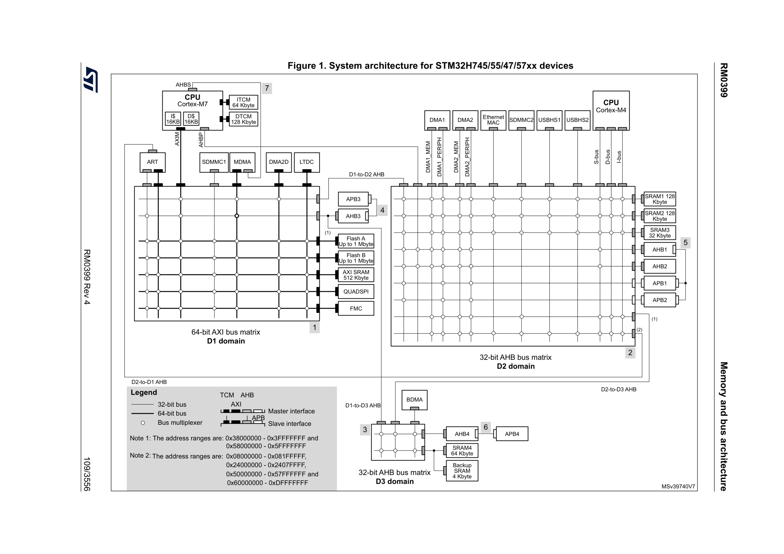
When working with the STM32H7, the primary architectural logic to consider is the distributed memory and bus design. Unlike simpler MCUs where memory is a single uniform block, the H7 is split into distinct domains (D1, D2, D3) connected by a complex bus matrix. To prevent system stalls or jitter, a developer must surgically place data based on its consumer. High-speed application code and graphics should live in D1-domain AXI SRAM for maximum CPU performance. Peripheral data — such as UART or SAI buffers — should ideally reside in D2-domain SRAM1/2, allowing DMA controllers to move data without competing for the CPU’s local buses. Ignoring this spatial logic leads to bus contention, where a high-speed peripheral can effectively starve the CPU, causing real-time deadlocks often seen in complex multitasking projects.
Why D3 is the low-power domain
Imagine the chip in deep sleep. The user has put the device down, the screen is off, the M7 is halted. You still want the device to wake on a specific event — a button press, a wake-word, a real-time clock alarm, an audio level rising above threshold. You don’t want to run a 480 MHz Cortex-M7 to do that, because it would drain the battery in hours.
ST’s answer is D3. Its peripherals are exactly the ones useful for “listen for something while everything else sleeps”: RTC for time-of-day wakeups, LPUART and LPTIM for low-power comms and timing, SAI4 for audio input, ADC3 for analog sampling. Its DMA controller (BDMA) is small, sips power, and can only access its own SRAM4 — that’s not a limitation but a design constraint that lets ST keep BDMA’s clock tree small enough to leave running while the rest of the chip is off. When the wake event happens, D3 kicks D1 and D2 back to life and hands the data off. On this project D3 sits unused most of the time, but the architectural option is there.
Why D2 is the peripheral domain
D2 is where the workhorses live: serial buses, audio interfaces, SD card, USB, Ethernet. These peripherals need DMA to keep up with sustained throughput — moving an audio sample every 62.5 µs, an SD card sector every few microseconds, an Ethernet frame every microsecond at line rate. The CPU can’t be in that loop; DMA1 and DMA2 are.
ST gave D2 its own SRAM (SRAM1/2/3, totalling 288 KB) so that peripheral DMA can complete without ever touching the D1 AXI bus. That keeps the M7 free to run application code in parallel, and avoids contention between (say) the LCD scanning out pixels from AXI and DMA1 dropping audio samples into SRAM1. The peripheral domain can also wake the chip more autonomously than D1 — useful for “USB inserted” or “Ethernet packet arrived” wake patterns.
Why D1 is the core domain
D1 is the M7 itself: ITCM for instructions, DTCM for stack/data, and AXI SRAM as the main working RAM. AXI is reachable by every DMA master in the system, which is exactly what you want for buffers that multiple subsystems touch — like a framebuffer that the CPU writes, DMA2D blits into, and LTDC scans out of. Putting AXI in D1 means it inherits the M7’s high-speed clock. Putting the framebuffer in D1 AXI rather than external SDRAM removes one major source of FUIF (LCD FIFO underrun): the LCD controller doesn’t have to fight the SDRAM controller’s refresh cycles for bus access.
The AHB bus matrix — what stitches it all together
The H7’s bus matrix is a crossbar switch. Each master (CPU AXI port, M4 instruction/data ports, DMA1, DMA2, BDMA, MDMA, DMA2D, LTDC, SDMMC IDMA, JPEG codec, etc.) has a connection point. Each slave (every SRAM region, every peripheral register block, FMC, QSPI) has another. The matrix routes any master to any reachable slave, with hardware arbitration when two masters want the same slave at the same time.
The key practical fact: not every master can reach every slave. DMA1/2 live in D2 and can reach D1 AXI plus all D2 SRAMs, but not D3 SRAM4. BDMA lives in D3 and can only reach D3 SRAM4. MDMA is the exception — it has connections into every domain — which is why it’s the right tool when you need to move data between domains. If you put a DFSDM DMA buffer in D3 SRAM4 expecting DMA1 to fill it, the build will compile, the link will succeed, the chip will boot, and the buffer will just stay zero forever because DMA1 cannot reach that address. There is no error, no warning, no diagnostic. That’s the kind of bug placement awareness prevents.
MDMA — the special DMA
MDMA is worth its own paragraph. Unlike DMA1, DMA2 and BDMA, which are tied to specific peripheral request lines and live within a single domain, MDMA is a memory-to-memory engine that can read from any source in any domain and write to any destination in any other. It’s designed for bulk transfers — copying decoded JPEG frames from SDRAM into AXI, copying audio blocks from D2 SRAM into D1 AXI for cache-coherent processing, copying flash assets into RAM during boot.
MDMA has more sophisticated channel features than DMA1/2: it can do 2D transfers (useful for image regions), endian conversion on the fly, and complex linked-list descriptors. It’s the right hammer when “copy big block, don’t care which CPU or DMA touches it” is what you need. The trade-off is higher per-transfer setup cost, so it’s not the right choice for moving 16 bytes between adjacent SRAMs every millisecond — for that, DMA1/2 are leaner.
5. Software Component Block Diagram — Audio + UART + LCD Pipeline
Here’s how the moving parts of this specific project relate on the STM32 side. The audio path lives entirely in D2. The UART RX queue is in D1 AXI. RTT diagnostic buffers live in D3 SRAM4. LCD framebuffer is in D1 AXI. Tasks have priorities that let VoiceRecTask (32) preempt almost everything, with UARTReceiveTask (26) close behind, and TouchGFXTask (High, ~24) rendering the UI in the background. The right-hand “Wi-Fi companion” branch in the diagram is intentionally simplified — what matters for this post is the STM32-side UART RX / TX path and where its buffers live.
Table 5.1 — Audio capture pipeline
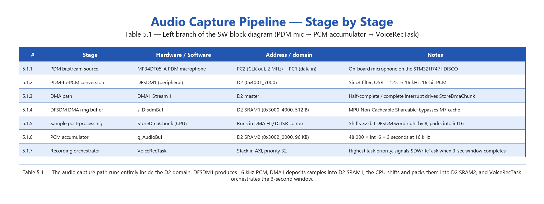
Table 5.2 — UART RX pipeline
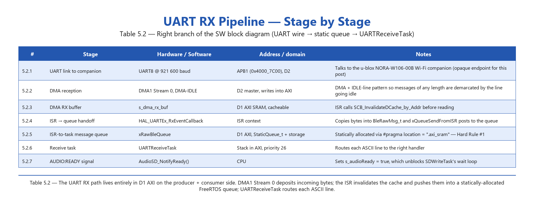
Three things are worth pointing out. One: the audio path lives entirely in D2 — DFSDM (D2 peripheral), DMA1 (D2 DMA), s_DfsdmBuf (D2 SRAM1), g_AudioBuf (D2 SRAM2). Zero AXI bus involvement during recording, so the LCD scanning AXI doesn’t interfere with audio capture and vice versa. Two: the UART RX queue is in D1 AXI — both producer (ISR) and consumer (UARTReceiveTask) are CPU code, never DMA, so the queue doesn’t need to be in a DMA-reachable region. AXI is fine and sits next to the DMA buffer (s_dma_rx_buf) the ISR reads from. Three: RTT buffers live in D3 SRAM4 — not because of any hard requirement (the M7 reaches D3 over the bus matrix without issue) but because AXI was already 97% full and SRAM4 was completely unused. Section attribution makes this kind of relocation a single-line change.
6. Memory Placement Audit — Reading the IAR ‘.map’ File
Understanding the STM32H747 memory architecture is essential before assigning any buffer or RTOS object to a region. The .map file in IAR is the final, comprehensive report generated by the linker after each build, and it is the source of truth for the physical location of every function and variable in the MCU’s memory. While the .icf file acts as the blueprint or plan, the .map file shows the actual execution: it details exactly which address was assigned to every symbol, its size, and which memory section it belongs to.
For an STM32H7 developer, this is the most essential tool for verifying that placement was successful. It allows you to confirm that DMA buffers are sitting in SRAM1 (and not accidentally in DTCM, which is inaccessible to DMA), or to ensure that your static queues are properly located in the AXI SRAM as intended. Analysing the map file is crucial for identifying memory hogs, preventing overflow, and resolving complex bus contention issues by verifying a total physical separation between different system variables.
How the IAR `.map` file helps during development
The IAR .map file is more than a passive report — it’s the developer’s most reliable debugging document. On every build, the linker writes a complete inventory of the firmware to EWARM/<Config>/List/<Project>.map. This includes the absolute address and size of every symbol, the section each symbol was placed into, the object file it came from, and a region-by-region summary of free space. Three habits make it indispensable on this project. First, grepping for a specific symbol immediately tells you whether the linker honoured your placement intent — if you wrote #pragma location = “.sram1” and the symbol appears at 0x24050000, you know the section directive was wrong or missing in the .icf. Second, the placement summary at the top of the file shows total bytes used per region, which lets you see how close you are to a Lp011: section placement failed error before it actually fires. Third, diffing the .map between two builds is the fastest way to catch unintended growth — a refactor that adds 25 KB to AXI .bss will show up as a region-summary delta even if no code change “looked” memory-related. On this project, the .map was the diagnostic that caught the LCD re-enable overflow, the rtos_trace dead-storage cost, and the RTT-buffer-in-AXI inefficiency that we eventually moved to D3 SRAM4.
The `#pragma location` directive
#pragma location is an IAR-specific compiler instruction used to force the placement of a variable or function at a specific memory address or within a named memory section defined in the .icf file. Unlike standard variable declarations where the compiler chooses the location automatically, this directive gives the developer precise control over the hardware mapping. In high-performance systems like the STM32H7, it is a critical tool for ensuring that DMA buffers are placed in peripheral-accessible RAM (like SRAM1) and that high-frequency RTOS objects are stored in fast-access memory (like AXI SRAM). By using this pragma, you move away from the unpredictability of a dynamic heap and toward a deterministic, hard-coded memory layout that prevents bus contention and ensures system stability.
What `#pragma location` actually does — theory, motivation, and what it solves
By default, the C/C++ compiler is allowed to put your variables anywhere in the writable memory regions the linker has been given (.data, .bss, .noinit). The compiler’s only obligation is to honour storage class (static / extern / automatic) and alignment. Where in RAM each variable ends up is decided by the linker after seeing every object file, and it can shift on every build as the size and order of symbols changes. For a single-region MCU with one flat SRAM this is fine; nothing depends on the absolute address. For a multi-domain MCU like the STM32H7, where the same variable behaves differently depending on whether it lands in D1 AXI, D2 SRAM1, D3 SRAM4, or DTCM, “anywhere” is not an acceptable answer.
#pragma location is the IAR compiler’s mechanism for removing the linker’s freedom over a specific variable’s placement and pinning it to either an absolute address or a named section that the .icf linker script maps to a specific physical region. It’s the IAR-native equivalent of GCC’s __attribute__((section(…))), with the additional ability to specify a literal address as the destination. Officially documented in the IAR C/C++ Development Guide for Arm (EWARM_DevelopmentGuide.ENU.pdf) — search for “pragma directives” → “location” — and the IAR Linker and Library Tools Reference Guide (EWARM_LinkerGuide.ENU.pdf). Both ship with every EWARM install in the doc/ subdirectory; the latest revisions are also downloadable from the IAR documentation portal at [www.iar.com/knowledge/support/technical-documentation/](https://www.iar.com/knowledge/support/technical-documentation/) (search “EWARM Development Guide”).
The directive has two forms.
Form 1 — placement in a named section:
#pragma location = “.my_section”
static uint8_t my_buffer[1024];
The linker then needs a matching directive in the .icf script that maps .my_section to a memory region:
place in SRAM1_region { section .my_section };
This is the form to use when the goal is “land in a particular domain” without caring about the exact byte address. The linker still chooses the precise offset inside the region, but it’s constrained to that region.
Form 2 — placement at an absolute address:
#pragma location = 0x30004000
static __no_init uint32_t hw_pinned_buffer[128];
The variable lands at exactly that address. The linker treats it as a “do not place anything else here” reservation. This form is used for buffers tied to specific hardware constraints (e.g., DMA buffers a peripheral expects at a fixed location, or alignment-sensitive buffers that need a known boundary).
Why use it — what the directive solves. Three problems disappear the moment a critical buffer carries a #pragma location:
- Silent placement drift across builds. Without the pragma, a refactor that adds 200 bytes of .bss somewhere unrelated can shift every subsequent symbol forward by 200 bytes. If your DMA buffer was sitting comfortably at 0x24050000 last build and now lives at 0x240500C8, the firmware still works — but the MPU region you set up for it doesn’t cover the new address. With #pragma location, the address is stable across builds and that whole class of “worked yesterday, broken today” goes away.
- Domain-correctness verified at link time, not runtime. The .icf script knows which sections map to which physical regions. A #pragma location = “.sram1” directive in source plus a place in SRAM1_region { section .sram1 } in the .icf together guarantee, at link time, that the buffer ends up in D2 SRAM1 — not somewhere DMA1 can’t reach. The compiler won’t catch a missing pragma; the linker won’t catch it either; but a present pragma plus matching .icf rule is a contract the toolchain enforces.
- Predictable cohabitation in the same region. When several related buffers all need to share the same domain (the DMA target buffer, the queue control block, the queue storage backing it), giving them all the same named-section pragma groups them physically together in RAM. Cache lines, MPU regions, and address ranges become reasoning units instead of accidents.
What it does NOT solve. #pragma location does not move task stacks (those come from the FreeRTOS heap, wherever that lives — see Hard Rule on static allocation), does not fix cache coherency on its own (that needs the MPU or explicit cache maintenance), and does not protect against a typo in the section name (a section name with no matching .icf placement silently falls back to default .bss — the linker won’t warn). Verification in the .map file after every build is the practical safeguard against all three.
In the body of this post you’ll see #pragma location applied to the DFSDM DMA ring (absolute address in D2 SRAM1), the PCM accumulator (absolute address in D2 SRAM2), the UART RX DMA buffer and its FreeRTOS queue control block (named .axi_sram in D1 AXI), and the SEGGER RTT buffers (named .sram4_rtt in D3 SRAM4). Each placement is a deliberate decision documented in a comment next to the declaration, and each is verifiable in the .map.
What ended up where (the audit by domain)
D1 DTCM (`0x20000000`, 128 KB) — CSTACK (8 KB) and the unused C-runtime HEAP (4 KB). No DMA can reach DTCM; the M7 stack is safe by construction. ~116 KB free.
D1 AXI SRAM (`0x24000000`, 512 KB) — TouchGFX_Framebuffer at the start (281 KB), ucHeap for FreeRTOS (96 KB), HAL handles, queue control blocks, the UART RX DMA buffer at 0x2407CA80 (128 B). About 13 KB free — tight.
D2 SRAM1 (`0x30000000`, 128 KB) — s_DfsdmBuf at 0x30004000 (512 B). The other ~127 KB is free and available for future audio extensions or relocated heaps.
D2 SRAM2 (`0x30020000`, 128 KB) — g_AudioBuf at 0x30020000 (96 KB, 48000 × int16 PCM). The remaining ~32 KB is free.
D3 SRAM4 (`0x38000000`, 64 KB) — s_upBuf for SEGGER RTT (16 KB), s_downBuf (16 B), _SEGGER_RTT control block at 0x38000010 (96 B). The rest is unused.
External SDRAM (`0xD0000000`, 32 MB) — JPEG decode intermediates (s_ycbcrBuf, s_rgb888Buf, s_rgb888Scaled) totalling ~5.4 MB. Plenty of headroom.
7. Collision Audit
Placement audits are necessary but not sufficient. Once every buffer is mapped to a domain, you have to check that the right master can reach each one and that adjacent buffers can’t trample each other. A few specific checks I run after every significant build:
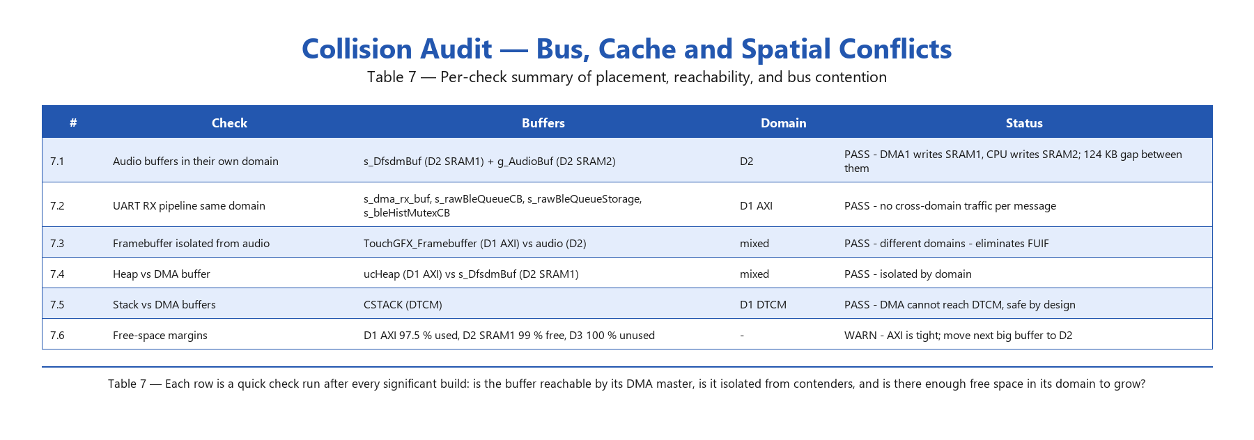
Table 7 — Description of each row:
7.1 — Audio buffers in their own domain. The DFSDM DMA ring sits in D2 SRAM1, the PCM accumulator in D2 SRAM2. DMA1 (a D2 master) writes the ring directly; the CPU later shifts samples into the accumulator. Both buffers stay inside D2, so the audio path never competes with the LCD’s traffic on the D1 AXI bus. The 124 KB gap between them is empty headroom in SRAM1 for future audio features.
7.2 — UART RX pipeline in a single domain. Every piece of state along the receive path — the DMA target buffer, the FreeRTOS queue control block, the queue storage, and the history-mutex control block — lives in D1 AXI SRAM. Both producer (the DMA-completion ISR) and consumer (UARTReceiveTask) are CPU code, so no cross-domain bus traffic happens for each received message. This was the fix for a regression where the queue used to be dynamically allocated and moved across domains as the heap moved.
7.3 — Framebuffer isolated from audio. The TouchGFX partial framebuffer sits at the start of D1 AXI; the audio path is entirely in D2. LTDC scans AXI as a D1 master; DMA1 fills SRAM1 as a D2 master. The two paths never collide on the same bus segment, which is what eliminates LCD FUIF (FIFO underrun) interrupts during heavy audio capture.
7.4 — Heap vs DMA buffer. The FreeRTOS heap sits in D1 AXI; the DFSDM DMA ring sits in D2 SRAM1. Earlier in the project’s life the heap was placed in D2 SRAM1 immediately after the DFSDM buffer, and task-creation logic stalled the audio pipeline. Moving the heap to AXI removed the contention. The general rule: never put a CPU-heavy structure adjacent to an active DMA buffer in the same MPU region.
7.5 — Stack vs DMA buffers. CSTACK is in DTCM. No DMA master on the H7 can reach DTCM — it is tightly coupled to the M7 alone. As a consequence, no stray DMA transfer can ever corrupt the stack regardless of pointer bugs or misconfigured peripherals. This is one of the strongest reasons to keep the M7 stack out of AXI.
7.6 — Free-space margins. D1 AXI sits at 97.5 % occupied — there is ~13 KB of headroom. D2 SRAM1 is almost entirely empty (127 KB free). D3 SRAM4 is mostly empty (~48 KB free after the RTT buffers). When the next big buffer needs adding, the answer is “D2 SRAM1 or D3 SRAM4” — and section attribution makes that a one-line change.
A previous configuration on this project had the FreeRTOS heap adjacent to the DFSDM buffer in the same MPU region. Task-creation logic was stalling the audio pipeline because of competing bus traffic, and the bug was non-deterministic — sometimes audio came through, sometimes the pipeline stalled until the next reset. Moving the heap to AXI SRAM in D1 eliminated the contention completely. That issue is now resolved, but it’s a textbook example of why “default placement” should never be trusted for DMA-adjacent buffers.
Collision types and how we solved them
Three classes of collision can occur on an STM32H7 system, each with its own signature and its own fix. (1) Spatial overlap — two variables claim overlapping address ranges because the .icf doesn’t carve out their regions correctly. This is the loudest failure mode: the linker errors out with Lp011: section placement failed, the build refuses to complete, and you have an explicit shortfall in bytes to triage. Fix: rebalance the section directives in the .icf, or move a large buffer to a different domain via #pragma location. (2) Bus contention — two masters try to drive the same bus segment at the same time. Symptoms are non-deterministic: jitter in audio capture, LCD FUIF interrupts during heavy CPU work, missing UART bytes during long SDMMC writes. The fix is to move one of the contenders to a different domain. On this project, the LCD framebuffer in D1 AXI and the DFSDM ring in D2 SRAM1 share no buses on the critical path, so they can run concurrently at full rate. (3) Cache coherency collision — the CPU cache and a DMA controller hold conflicting views of the same memory location. This is described in detail in the cache section below. Symptoms look like random data corruption — the kind that survives across resets but disappears when you add a printf because the print changes the cache eviction pattern. The fix is either an MPU Non-Cacheable region for the buffer, or explicit SCB_CleanDCache_by_Addr / SCB_InvalidateDCache_by_Addr calls bracketing every DMA transaction. Recognising which class you’re facing is most of the diagnostic work: build-time errors are Type 1, performance-related symptoms are Type 2, “impossible” data values are usually Type 3.
The general principle: each domain should serve one and only one traffic class. Don’t mix CPU-intensive RTOS objects with peripheral DMA buffers in the same region. If you find yourself doing that, either move one of them or accept the contention will eventually bite you.
When to use D2 SRAM vs D1 AXI SRAM
There’s a recurring question that comes up on every new buffer: should this live in AXI or in D2 SRAM? Both are reachable from the CPU. Both are reachable from DMA1/2. The decision criteria are: (a) Who is the primary master? AXI is faster from the CPU side (fewer wait states, on the M7’s main bus), so put CPU-dominated data there. D2 is naturally adjacent to DMA1/2, so put peripheral-dominated data there. (b) How big is the buffer? Large buffers go to D2 because AXI is more contested (framebuffer, JPEG state, heap, queues, HAL handles all want AXI). A 96 KB audio accumulator in AXI would crowd everything else; the same buffer in D2 SRAM2 leaves AXI free. (c) Does it cross the bus matrix on every access? A buffer that the CPU touches once per frame and DMA touches 1000 times per second should be in the DMA’s domain (D2). A buffer the CPU touches 10000 times per second and DMA touches once should be in AXI. On this project the rule played out cleanly: framebuffer → AXI (LTDC scans it as a D1 master), heap → AXI (FreeRTOS API touches it on every task switch), DFSDM ring → D2 SRAM1 (DMA writes it continuously), PCM accumulator → D2 SRAM2 (CPU writes it once per DMA chunk, SDMMC reads it once per file). When in doubt, the master that wins arbitration most often dictates the region.
8. Where Each Buffer Class Belongs on STM32H747
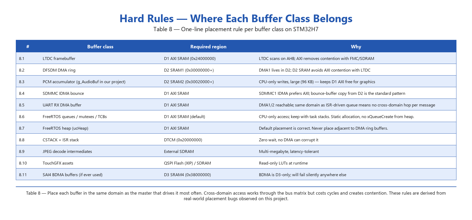
Table 8 — Description of each row:
8.1 — LTDC framebuffer in D1 AXI. The LTDC scans the framebuffer at line rate (in this project ~60 Hz × 800 × 480 × 3 bytes/pixel) and is a D1 master. Placing the framebuffer in AXI keeps that traffic inside D1; placing it in external SDRAM forces every scan to compete with the FMC controller’s refresh cycles, which is the textbook cause of LCD tearing (FUIF) on H7 designs.
8.2 — DFSDM DMA ring in D2 SRAM1. DMA1 is a D2 master. The DFSDM filter produces 32-bit samples that DMA1 deposits into the ring at 16 kHz. Keeping the buffer in D2 SRAM means DMA1 never crosses the bus matrix; the LCD on D1 AXI runs concurrently without contention.
8.3 — PCM accumulator in D2 SRAM2. A 96 KB buffer that the CPU writes once per DMA chunk and SDMMC reads once per file. Large buffers crowd AXI (which is already 97 % full with the framebuffer + heap); D2 SRAM2 has ample empty space. CPU access through the bus matrix is acceptable here because each access is infrequent.
8.4 — SDMMC IDMA bounce in D1 AXI. SDMMC1’s internal DMA prefers AXI as its destination. The PCM data lives in D2 SRAM2; SDWriteTask memcpys it into an AXI bounce buffer before issuing the SDMMC write. The bounce is the trade-off that lets us keep the big audio buffer in D2 while still using the AXI-friendly SD path.
8.5 — UART RX DMA buffer in D1 AXI. The UART RX DMA (DMA1, but reaching back into AXI) deposits incoming bytes here. Adjacent in AXI is the ISR-driven xRawBleQueue. Because both buffers are in the same domain, the ISR’s memcpy from DMA buffer to queue storage costs no cross-domain bus traffic.
8.6 — FreeRTOS queues, mutexes, TCBs in D1 AXI. All CPU-side data, accessed every task switch and every API call. Default .bss placement in AXI is correct. Critical caveat: queue and mutex storage must be statically allocated (xQueueCreateStatic, xSemaphoreCreateMutexStatic) — otherwise the storage lives wherever the heap is, and the heap can quietly move across builds.
8.7 — FreeRTOS heap in D1 AXI. The 96 KB ucHeap[] is the default for heap_4 and works correctly in AXI. The hard rule here is negative: never place the heap adjacent to a DMA ring buffer in the same MPU region. Earlier in this project’s life the heap drifted next to the DFSDM ring in D2 SRAM1, and task-creation operations would corrupt audio capture non-deterministically.
8.8 — `CSTACK` and ISR stack in DTCM. Zero wait states for the M7, and no DMA master can reach DTCM, so stack corruption from a stray DMA transfer is impossible by design. DTCM is the only place the M7 stack should ever live.
8.9 — JPEG decode intermediates in external SDRAM. The YCbCr and RGB888 working buffers for JPEG decoding total several megabytes — too big for any internal SRAM. SDRAM is fine here because the JPEG codec is latency-tolerant and the decode is offline (not real-time per scan line).
8.10 — TouchGFX assets in QSPI Flash or SDRAM. Fonts, bitmaps, and pre-rendered icons are read-only at runtime. QSPI Flash gives execute-in-place reads without consuming RAM; SDRAM is used when the asset is too big for QSPI or needs to be decompressed at boot.
8.11 — SAI4 BDMA buffers in D3 SRAM4 only. BDMA is the D3-local DMA controller and cannot reach D1 or D2 SRAM. If a SAI4-driven BDMA path is ever added to a project, its DMA buffer must be in D3 SRAM4. Putting it anywhere else compiles and links cleanly but produces zero data movement at runtime — a silent failure mode.
The pattern: place each buffer in the same domain as the master that drives it most frequently. Cross-domain access works through the bus matrix, but it costs cycles and creates contention. Putting things in their natural domain isn’t optimisation — it’s the path of least surprise.
9. Managing the Cortex-M7 L1 Cache on STM32H747
A quick refresher — what is a cache, and what types exist?
Before diving into the specific cache-management work the STM32H7 demands, it helps to ground the discussion in the general theory of CPU caches, because the H7 only exposes a subset of what a modern processor architecture offers and knowing what’s missing is as important as knowing what’s there.
A cache is a small, very fast memory placed between the CPU and main memory. Its job is to hide the latency of slower memory by keeping recently-used data and instructions close to the CPU. Every read miss costs full memory-access time; every cache hit costs a single CPU cycle. The bigger the gap between CPU speed and memory speed, the more performance a cache buys. On a 480 MHz Cortex-M7 reading from external SDRAM at ~50 ns per word, that gap is ~20× — caches matter.
Caches are usually organised in levels, numbered by their distance from the CPU pipeline. Each level is larger and slower than the one above it.
In addition to the level numbering, L1 is conventionally split along the von Neumann / Harvard line into two physically separate banks:
- I-cache (Instruction cache) — caches read-only instruction fetches from Flash or RAM-resident code. Never written by the CPU, so it has no dirty-line problem. Invalidation only matters when self-modifying code or runtime relocation moves instructions around.
- D-cache (Data cache) — caches load/store accesses to data. Can be either write-through (every write goes immediately to memory and is also kept in cache) or write-back (writes update the cache, and the dirty line is flushed to memory later). Write-back is faster but introduces the cache-coherency problems described in this section.
Where the Cortex-M7 fits in this picture. The Cortex-M7 core inside the STM32H747 has L1 only — and only L1. No L2, no L3. Specifically:
- L1 I-cache: 16 KB, 2-way set-associative, 32-byte lines.
- L1 D-cache: 16 KB, 4-way set-associative, 32-byte lines, write-back with read-allocate by default.
- No L2 unified cache — main memory is the next stop after an L1 miss.
- No MMU — memory protection is via the MPU (16 regions) which can change cacheability attributes per region but does not provide virtual-address translation.
This puts the H7 in a useful middle ground: it has the performance of a cached pipeline (which is why it can hit 480 MHz on commodity SRAM and Flash), but it doesn’t have the silicon area or the bus complexity of L2/L3 hierarchies. It also doesn’t have the cache-coherency hardware that multi-core application processors have for keeping caches in sync between cores. That coherency burden is yours to manage in software, and that’s what the rest of this section is about. By contrast, lower-end Cortex-M cores (M0, M0+, M3, M4) have no cache at all — every load and store goes straight to memory, which is why they cap out at much lower clock rates but never need any of the cache-maintenance discipline below.
Why managing the cache matters on STM32H747
Managing the L1 cache on the STM32H7 (Cortex-M7) is a mandatory requirement for system reliability. The core problem is a synchronisation gap between what the CPU sees and what the hardware actually does. To achieve high performance, the CPU reads and writes data to its local L1 D-cache rather than slower physical RAM. However, peripheral DMA controllers — such as those for UART, SAI, or Ethernet — bypass this cache entirely and talk directly to the RAM.
Write and read coherency failures
This mismatch creates two distinct failure modes. First, if the CPU writes data to a buffer, the bytes might only sit in the cache, leaving the DMA to transmit old data from the RAM — a “Write-Dirty” issue. Second, the DMA might update the RAM while the CPU continues to read stale values from its cache — a “Read-Stale” issue.
To address this correctly, you must either use the MPU to define specific DMA regions as Non-Cacheable, or manually perform Cache Maintenance operations: Clean (forcing cache data out to RAM before a DMA transmit) and Invalidate (clearing the cache so the CPU is forced to read fresh data from RAM after a DMA receive). Failure to do so results in random, non-deterministic data corruption that can silently break communication protocols and audio streams. Worst of all, these bugs appear as random software glitches rather than the hardware configuration errors they truly are.
In practice on this project, the audio buffers (s_DfsdmBuf and g_AudioBuf) live in MPU-configured Non-Cacheable Shareable regions of D2 SRAM. That means the M7 reads and writes them straight through to RAM, no cache involvement, no invalidate/clean dance required. The performance hit is small (audio is slow data), and the simplification is large. For the UART RX buffer in AXI, where caching is on, the ISR does SCB_InvalidateDCache_by_Addr(s_dma_rx_buf, BLE_DMA_BUF_SIZE) immediately before reading the bytes DMA just wrote. The 32-byte alignment requirement is non-negotiable; pad your buffer declarations with __attribute__((aligned(32))) and size them in 32-byte multiples.
Cache considerations across the project
There are three patterns that recur for cache management on this architecture and it’s worth being explicit about each. Pattern A — Non-Cacheable MPU region for DMA buffers. This is the simplest and most foolproof: declare an MPU region covering the buffer’s address range with the Non-Cacheable and Shareable attributes, and the CPU bypasses the cache for every access to that region. No Clean, no Invalidate, no alignment headaches. The cost is slightly slower CPU access (because every read/write hits RAM directly), but for audio buffers updated at 16 kHz this is invisible. We use this for s_DfsdmBuf and g_AudioBuf in D2 SRAM. Pattern B — Cacheable region with explicit maintenance. For high-throughput DMA paths where bypassing the cache would actually hurt (e.g., a buffer the CPU also processes heavily), keep it cacheable but bracket every DMA transaction with SCB_CleanDCache_by_Addr before a transmit and SCB_InvalidateDCache_by_Addr before reading after a receive. We use this for the UART RX path: the buffer is in AXI, caching is on, the ISR invalidates the cache lines immediately before reading the DMA-deposited bytes. The discipline must be applied at every call site; missing a single invalidate produces intermittent corruption. Pattern C — Cache-coherent regions (TCM and the AXI-cache mode where applicable). DTCM and ITCM are by construction outside the cache hierarchy — no Clean, no Invalidate, no MPU configuration needed. This is why the M7 stack lives in DTCM: cache coherency is just not a concept that applies there. For framebuffers in AXI, we rely on the LTDC controller’s burst-read semantics combined with the CPU’s write-back cache being flushed on each DMA2D blit boundary; TouchGFX’s framework handles the discipline transparently. The general decision tree: small DMA buffers → Pattern A; high-throughput CPU+DMA shared buffers → Pattern B; CPU-private fast data → DTCM / Pattern C. Pick one pattern per buffer, document the choice in a comment next to the declaration, and never mix patterns within a single buffer.
Why cache coherency is needed at all — and what it solved
The cache exists because main memory is too slow for a 400 MHz CPU pipeline. Without it, every load and store would stall the M7 by tens of cycles waiting for RAM. So the cache is not an optional optimisation — it’s the reason the M7 can run at 400 MHz on commodity SRAM in the first place. But the moment you turn the cache on, you create a second view of memory: the CPU sees what its cache holds, while every other bus master (DMA controllers, LTDC, SDMMC IDMA, JPEG codec, MDMA, the second core if it were used) sees the actual contents of RAM. Those two views are kept consistent automatically only between the CPU and its own cache. They are not kept consistent between the cache and any other master. That gap is the cache-coherency problem in a single sentence: the hardware that gives you 400 MHz throughput also gives you two divergent versions of the same bytes, and the architecture provides no automatic mechanism to reconcile them.
Cache-coherency operations exist to close that gap manually. There are two directions to consider, and both matter. In the DMA-to-CPU direction (peripheral receives data, CPU reads it): a DMA controller writes bytes directly to physical RAM, bypassing the cache. The CPU then issues a read at the same address, but the cache may still hold the previous contents of that line — pre-DMA, stale. Without an Invalidate operation before the CPU read, the load hits the cache and returns the old data. The Invalidate marks the relevant cache lines as empty, forcing the next read to go all the way to RAM and pick up the DMA-deposited bytes. In the CPU-to-DMA direction (CPU prepares data, peripheral transmits it): the CPU writes to a buffer; in write-back mode those writes sit in the cache and have not yet been pushed to RAM. If the DMA reads the buffer before the cache is flushed, the peripheral transmits stale RAM contents instead of the CPU’s intended bytes. The Clean operation forces dirty cache lines back out to RAM, so a subsequent DMA read sees the up-to-date version.
What cache coherency operations actually solved on this project. Two concrete bug classes disappeared once the patterns above were in place. First, the UART RX silent-loss bug. Before the explicit SCB_InvalidateDCache_by_Addr was added to the receive-complete ISR, the wire and the J-Link probe both confirmed that bytes were arriving at the DMA buffer in AXI — but the CPU was reading zeros for entire messages. The cache was holding the line’s pre-DMA state (which happened to be the zero-filled .bss initialisation), and the CPU’s reads hit the cache instead of the freshly-written RAM. Adding the Invalidate immediately before the read fixed it. The fix wasn’t a code change in the sense of new logic — it was the explicit acknowledgement that the cache and the DMA had two views, and the ISR had to reconcile them at the right instant. Second, the audio capture corruption that would have followed. Without the MPU Non-Cacheable Shareable region covering s_DfsdmBuf at 0x30004000, the DFSDM DMA would have written 32-bit samples into RAM every 62.5 µs while the CPU’s cache held stale lines from the previous half-buffer. The StoreDmaChunk reads in the half-complete and complete callbacks would have read alternating real-and-stale samples — audible as a sample-rate periodic distortion. By making the region Non-Cacheable at the MPU level, we sidestepped the problem entirely; the CPU never caches those addresses, so there is no second view to reconcile.
In both cases, the operations didn’t add functionality — they prevented the silent corruption that would have come from the cache’s existence. Cache coherency is the cost of having a fast cache in the first place. The art of designing on the M7 is choosing, per buffer, whether to pay that cost in explicit per-callsite Clean/Invalidate calls (Pattern B), in an MPU region attribute that bypasses the cache entirely (Pattern A), or in a placement that puts the buffer outside the cache’s reach to begin with (Pattern C in DTCM). Whichever pattern you pick, the underlying truth is the same: on the H7, every byte that crosses between a CPU and a DMA master needs an explicit coherency decision, and skipping that decision is how silent data corruption enters a real-time system.
10. IAR Section Attribution Cheat Sheet — ‘# pragma location’ Syntax
Example — typical placements from this project (variable names are illustrative; pick your own naming for your own project):
/* Example: default .bss/.data — goes to D1 AXI SRAM by linker default */
static uint32_t g_counter;
/* Example: explicit AXI placement (rare, but documents intent) */
#pragma location = “.axi_sram”
static StaticQueue_t s_queueCB;
/* Example: D2 SRAM1 — DMA1/DMA2 reachable */
#pragma location = “.sram1”
static uint8_t s_dmaBuf[256];
/* Example: D2 SRAM2 — DMA1/DMA2 reachable */
#pragma location = “.sram2”
static int16_t s_audioBlock[8192];
/* Example: absolute address — for hardware-fixed buffers like the DFSDM ring */
#pragma location = 0x30004000
static __no_init uint32_t s_DfsdmBuf[128];
For the named-section approach to work, the .icf must define each section’s region. Example `.icf` snippet:
define region SRAM1_region = mem:[from 0x30000000 to 0x3001FFFF];
place in SRAM1_region { section .sram1 };
Without that, the named section silently falls back to default .bss placement, which is usually D1 AXI. I had a buffer attributed to a section name .dma_buf that “worked” for months because AXI happened to be DMA-reachable — but it was placed by accident, not by design. A later refactor moved adjacent symbols, the silently-misplaced buffer shifted with them, and a regression appeared. Section attribution is only protection if the .icf enforces it.
11. References
Official STMicroelectronics documentation (all available on st.com)
All of the application notes (AN) and reference manuals (RM, UM) below are published by STMicroelectronics on their official website (www.st.com). Each document is downloadable for free; search the document number on the ST site to get the latest revision.
- AN4861 — LCD-TFT display controller (LTDC) on STM32 MCUs (STMicroelectronics application note). FUIF / FIFO underrun causes, framebuffer bandwidth math, recommended memory placement for LTDC scan-out. Available at st.com.
- AN4891 — STM32H7 system architecture and performance (STMicroelectronics application note). The canonical reference for the H7’s bus matrix, the three power domains, and DMA-master reach across regions. Available at st.com.
- AN5215 — DMA controllers on STM32H7 MCUs (STMicroelectronics application note). Memory bandwidth, performance numbers, master arbitration. Available at st.com.
- AN5405 — Managing memory protection unit in STM32 MCUs and the related cache-coherency guidance (STMicroelectronics application note). Required reading for the Cortex-M7 D-cache + DMA interaction described in Section 9. Available at st.com.
- AN5027 — Interfacing PDM digital microphones using STM32 MCUs (STMicroelectronics application note). PDM clock and decimation pairing, mic-clock physics, AN5027 §2.4.2 on the shared-source rule. Available at st.com.
- RM0399 — STM32H745/755 and STM32H747/757 advanced Arm-based 32-bit MCUs reference manual (STMicroelectronics reference manual). Chapter 2 (memory map), chapter 8 (RCC), the bus-matrix appendix, and chapter 60 (DBGMCU) are the relevant sections for this post. Available at st.com.
- UM2411 — STM32H7 SAI (serial audio interface) (STMicroelectronics user manual). PDM input mode, SAI4 register-level detail. Available at st.com.
Tool-vendor documentation
- SEGGER RTT documentation (SEGGER Microcontroller) — wire protocol, control-block layout, host tools. Available at segger.com.
- SEGGER J-Link / J-Trace User Guide (UM08001) (SEGGER Microcontroller) — J-Link Commander commands, SWO, RTT, scripted batch invocation. Available at segger.com.
- IAR C-SPY Debugging Guide (UCSARM-26) (IAR Systems) — macro language reference, cspybat invocation, lifecycle hooks. Available at iar.com.
- IAR Linker and Library Tools Reference Guide (IAR Systems) — .icf linker-config syntax, section placement, #pragma location Available at www.iar.com.
For the IAR-specific compiler syntax (#pragma location, @ placement operator, .icf directives), the IAR C/C++ Development Guide ships with every EWARM installation under the doc/ subdirectory.
12. Conclusion
Five rules cover most of the placement decisions on STM32H747:
- To achieve a deterministic, high-performance STM32H747 system, you must place every buffer in the specific memory domain owned by the Bus Master that uses it . for example: DFSDM in D2 means audio buffers in D2 SRAM. LTDC in D1 means framebuffer in D1 AXI.
- Enforce strict static allocation. Heap-allocated objects move when the heap moves; static objects have fixed addresses you can audit in the .map and inspect via C-SPY without instrumentation.
- Use mandatory IAR placement — `#pragma location`, the `@` operator, or section attributes — for every critical variable. Never let a critical buffer float in default .bss or .data.
- Minimise cross-domain bus traffic. Each domain serves one traffic class. Heap and DMA buffers don’t share a region. UART DMA buffer and its consumer queue stay in the same domain.
- Adopt zero-footprint debugging — ITM, SWO, and `cspybat` C-SPY macros — instead of printf. At 480 MHz, printf alters the system under test; ITM doesn’t.
- prevent collision on the “Highway “Bus – To prevent collisions between two peripherals (like audio and video) on the STM32H7, you must design for spatial isolation. The H7 uses a complex Multi-Layer Bus Matrix that allows multiple masters to access different memories at the same time—but only if they aren’t fighting for the same Memory region, “Slave” port.
Two cautions sit alongside the rules. Always define explicit MPU regions for every memory area accessed by DMA, marking them Bufferable / Non-Cacheable; without that, the CPU cache and the DMA controller will hold conflicting versions of the same data, and you’ll spend days hunting non-deterministic corruption. And always use Mutexes (not binary semaphores) for shared resources in a multitasking system, because Mutexes support priority inheritance and prevent lower-priority tasks from inadvertently blocking higher-priority ones.
The practical takeaway: memory placement on H7 is part of the design, not part of the optimisation pass. Treat each new buffer like you treat each new task — give it a name, a domain, a reason, and a verified location in the .map — and the worst class of “works on Tuesday, breaks on Wednesday” bugs goes away.
13. Related Reading on the Sightsys Engineering Blog
If you found this STM32H747 memory architecture deep-dive useful, you’ll likely find the following companion posts on the Sightsys blog directly relevant:
- Debugging STM32 with cspybat and C-SPY Macros — . Covers macro language syntax, lifecycle hooks, the IAR project setup, and worked examples of automated post-build probes.
- ARM CoreSight Debugging on Cortex-M7 – Silicon foundation to debug any Cortex-Mx device.
14. Call to Action
If you’re building an STM32H7 product and hitting any of the symptoms described in Section 1 — audio jitter, LCD tearing, silent DMA corruption, FreeRTOS queue weirdness — the Sightsys engineering team works on this class of problem for a living. We help product teams from start-ups to OEMs design memory architectures, debug bus-contention issues, integrate TouchGFX cleanly, and bring STM32H7 designs to production.
Built and debugged with IAR Embedded Workbench 9.70.2 (`cspybat` 9.4.6.1706), SEGGER J-Link V9.34, on the STM32H747I-DISCO board.
Sightsys engineering. Estimated reading time: 18-22 minutes.