


")


")

ARM CoreSight Debugging on Cortex-M7
ARM CoreSight debugging is the silicon foundation behind every breakpoint, variable watch, SWO printf, and instruction trace you use in IAR or SEGGER tools. Every time you debug a Cortex-M chip, you’re using ARM CoreSight debugging — whether you realize it or not. CoreSight is the standardized debug and trace infrastructure that ARM bakes into every Cortex-M processor, from the tiniest M0 to the dual-core M7 in the STM32H747.
Probes like the IAR I-jet, SEGGER J-Link, SEGGER J-Trace, and IAR I-jet Trace are not magic — they are simply hardware adapters that talk to the CoreSight blocks already sitting inside your MCU. The probe drives the SWD or JTAG pins; CoreSight does the actual work.
Why does this matter for developers? Because once you understand what’s behind the curtain, you stop treating the debugger as a black box. You can write your own lightweight tracing (ITM stimulus ports), benchmark code paths down to the CPU cycle (DWT cycle counter), diagnose HardFaults without guessing (SCB fault registers), and configure trace output for tools like J-Trace or I-jet Trace (TPIU + ETM) — all by writing directly to memory-mapped registers that cost zero RAM and zero flash.
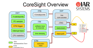
This reference walks through the full CoreSight memory map at 0xE0000000–0xE00FFFFF as it appears on the STM32H747 Cortex-M7 core, explains what each block does, what you can extract from it during a debug session, which probe uses it, and shows the exact registers we touch in our own project.
The CoreSight debug & trace region occupies the top of the ARM Cortex-M fixed memory map at 0xE0000000–0xE00FFFFF (1 MB, vendor-independent). Every Cortex-M device (M0 through M7) has these blocks at identical addresses. None of this region consumes your RAM or Flash — it is hardwired silicon.
The ARM CoreSight Debugging Block Map
┌─────────────────────────────────────────────────────────────────────┐
│  Address Range            Block    Full Name                        │
├─────────────────────────────────────────────────────────────────────┤
│  0xE0000000 – 0xE0000FFF  ITM      Instrumentation Trace Macrocell  │
│  0xE0001000 – 0xE0001FFF  DWT      Data Watchpoint & Trace          │
│  0xE0002000 – 0xE0002FFF  FPB      Flash Patch & Breakpoint         │
│  0xE0003000 – 0xE000CFFF  —        Reserved                         │
│  0xE000D000 – 0xE000DFFF  —        Reserved                         │
│  0xE000E000 – 0xE000EFFF  SCS      System Control Space             │
│                             ├─ SysTick   0xE000E010                 │
│                             ├─ NVIC      0xE000E100                 │
│                             ├─ SCB       0xE000ED00                 │
│                             └─ MPU       0xE000ED90                 │
│  0xE000F000 – 0xE000FFFF  —        Reserved                         │
│  0xE0040000 – 0xE0040FFF  TPIU     Trace Port Interface Unit (SWO)  │
│  0xE0041000 – 0xE0041FFF  ETM      Embedded Trace Macrocell         │
│  0xE0042000 – 0xE00FEFFF  —        Reserved                         │
│  0xE00FF000 – 0xE00FFFFF  ROM      ROM Table (debugger discovery)   │
└─────────────────────────────────────────────────────────────────────┘
Understanding this map is the foundation of effective ARM CoreSight debugging.
Which Probe Uses Which Block?
Different debug probes light up different parts of the CoreSight infrastructure. Knowing which block your probe relies on helps you pick the right tool — and explains why some features only work with certain hardware.
| Probe | Connection | CoreSight Blocks Used | What You Get |
|---|---|---|---|
| IAR I-jet | SWD + SWO | SCS, FPB, DWT, ITM, TPIU | Breakpoints, watchpoints, printf over SWO, cycle counting |
| SEGGER J-Link | SWD + SWO | SCS, FPB, DWT, ITM, TPIU | Same as I-jet, plus RTT (uses RAM, not CoreSight) |
| SEGGER J-Trace | SWD + 4-bit Trace Port | All of the above + ETM | Full instruction trace + streaming trace to PC |
| IAR I-jet Trace | SWD + 4-bit Trace Port | All of the above + ETM | Full instruction trace — every executed instruction recorded |
The key distinction comes down to how much of the trace bus the probe can read. I-jet and J-Link use only the single-pin SWO output (driven by TPIU), so they can stream ITM software events and sampled PC values, but cannot capture every instruction. J-Trace and I-jet Trace add a 4-bit parallel trace port that connects to the ETM block, giving you full instruction-level history — invaluable for tracking down rare bugs that disappear under a breakpoint. J-Trace additionally supports streaming trace continuously to the host PC’s RAM/disk, which lets you record much longer trace windows than the on-chip ETB can hold.
The STM32H747 DISCO board only routes SWO, so ETM-based trace is not available there — you’d need a board that exposes the TRACECLK + TRACEDATA[3:0] pins. Choosing the right probe is the first practical decision in ARM CoreSight debugging.
ITM — Instrumentation Trace Macrocell (0xE0000000)
What it does
The ITM is essentially a one-way mailbox from your firmware to the debugger. It exposes 32 “stimulus ports” — each is a 4-byte memory-mapped register. When you write to one, the ITM packages your data with a port ID and a timestamp, hands it to the TPIU, which serializes it out the SWO pin to the debug probe. The probe forwards it to the IDE, which displays it in a terminal window.
What you can get from it in a debugging session
printf-style debug output without a UART. The classic use case. IAR’s Terminal I/O window and SEGGER’s SWO Viewer both display ITM port 0 as a text stream. No UART pins, no DMA, no driver — justputcharwrites toITM->PORT[0].- Lightweight event tracing in time-critical code. A single 32-bit write to a stimulus port costs ~7 CPU cycles. That’s cheap enough to instrument an ISR or a tight control loop without distorting timing.
- Multi-channel logging. With 32 independent ports, you can split your output: port 0 for human-readable text, port 1 for binary state machine events, port 2 for RTOS task switches, port 3 for sensor samples. The host filters by port ID.
- Cross-correlation with hardware events. ITM packets carry timestamps generated by the same DWT cycle counter your code reads, so software events line up with hardware-captured PC samples or watchpoint hits.
- Production-safe instrumentation. When no debugger is attached, stimulus port writes are silently discarded by the hardware. You can leave ITM calls in shipped firmware with zero side effects.
Register map
| Offset | Register | Description |
|---|---|---|
| 0x000 | PORT[0] | Stimulus port 0 (u8 / u16 / u32 write) |
| 0x004 | PORT[1] | Stimulus port 1 ← our pipeline tokens |
| 0x008 | PORT[2] | Stimulus port 2 |
| … | … | (32 ports total, 4 bytes each) |
| 0x07C | PORT[31] | Stimulus port 31 |
| 0xE00 | TER | Trace Enable Register (1 bit per port) |
| 0xE40 | TPR | Trace Privilege Register |
| 0xE80 | TCR | Trace Control Register (global enable) |
| 0xFB0 | LAR | Lock Access Register |
| 0xFB4 | LSR | Lock Status Register |
Key rule: Before writing to a stimulus port, always check ITM->PORT[n].u32 != 0 — returns 0 when no debugger is attached (write is silently discarded = safe in release builds).
This is ARM CoreSight debugging at its most lightweight — a single 32-bit write.
DWT — Data Watchpoint & Trace (0xE0001000)
What it does
The DWT is the Cortex-M’s built-in performance counter and watchpoint engine. It provides a free-running 32-bit cycle counter that ticks at the CPU clock, plus up to 4 hardware comparators that can fire on data accesses to specific addresses. It’s the most underused block in the entire CoreSight family — most developers never touch it directly, but it answers questions that are nearly impossible to answer any other way.
What you can get from it in a debugging session
- Cycle-accurate benchmarking. Read
DWT->CYCCNTbefore and after a function. The difference is the exact number of CPU cycles consumed — including pipeline stalls, cache misses, and interrupts. On a 480 MHz STM32H747, one cycle = ~2 ns of resolution. No oscilloscope needed. - Data watchpoints — the variable-changed breakpoint. Configure a comparator on the address of a global variable, and the CPU halts the instant anything writes to it. This is how you find that one rogue function corrupting a shared buffer.
- Range watchpoints. Combine an address with a mask to watch an entire array, struct, or memory region. Useful for catching stack overflow corrupting a known-bad zone, or detecting writes outside a DMA buffer.
- Performance profiling counters. DWT exposes counters for CPI (cycles per instruction), exception overhead, sleep cycles, LSU cycles, and folded instructions. Sample these around a hot path and you get a hardware-level breakdown of where time actually goes.
- PC sampling for statistical profiling. The PCSR register exposes the current program counter. The debugger can sample it periodically over SWO to build a flat profile of where the CPU spends its time — without instrumenting your code.
Register map
| Offset | Register | Description |
|---|---|---|
| 0x000 | CTRL | Control (CYCCNTENA bit 0 = enable cycle count) |
| 0x004 | CYCCNT | Cycle Count Register |
| 0x008 | CPICNT | CPI Count Register |
| 0x00C | EXCCNT | Exception Overhead Count Register |
| 0x010 | SLEEPCNT | Sleep Count Register |
| 0x014 | LSUCNT | LSU Count Register |
| 0x018 | FOLDCNT | Folded Instruction Count Register |
| 0x01C | PCSR | Program Counter Sample Register |
| 0x020 | COMP0 | Comparator 0 (watchpoint address) |
| 0x024 | MASK0 | Comparator 0 Mask |
| 0x028 | FUNCTION0 | Comparator 0 Function |
Enable with: DWT->CTRL |= 1 (after CoreDebug->DEMCR |= TRCENA). The DWT is the cycle-counting heart of ARM CoreSight debugging.
FPB — Flash Patch & Breakpoint (0xE0002000)
What it does
The FPB is the silicon behind every breakpoint you set in IAR. When you click in the margin to add a breakpoint, the IDE doesn’t modify your flash — it loads the target address into one of the FPB’s comparators. When the CPU’s instruction fetch matches that address, the FPB inserts a BKPT instruction into the pipeline on the fly, halting the core. The original flash is never touched.
What you can get from it in a debugging session
- Up to 8 hardware breakpoints in flash. The Cortex-M7 FPB has 6–8 instruction comparators (vendor-configurable on STM32H747). That’s your hard limit — set a 9th breakpoint in IAR and it will either fail silently or fall back to a software breakpoint if the code is in RAM.
- Why your breakpoint sometimes “doesn’t hit.” If you’ve used all 8 slots, additional breakpoints are simply not armed.
- Flash patching for live code repair. The “Patch” half of FPB lets the debugger remap a flash word to a value in SRAM.
- Conditional breakpoints work because of FPB + DWT. When you set a conditional breakpoint, the IDE sets a real FPB breakpoint and evaluates the condition each hit.
Register map
| Offset | Register | Description |
|---|---|---|
| 0x000 | CTRL | Control (NUM_CODE = breakpoint count) |
| 0x004 | REMAP | Remap base address for flash patching |
| 0x008 | COMP0 | Comparator 0 (breakpoint address) |
| 0x020 | COMP6 | Comparator 6 |
You almost never write to FPB directly — the debugger owns it.
SCS — System Control Space and ARM CoreSight Debugging Faults (0xE000E000)
What it does
The SCS is the umbrella region that holds the four most important blocks for everyday firmware: SysTick (the RTOS timebase), NVIC (the interrupt controller), SCB (system control + fault status), and MPU (memory protection). Unlike ITM/DWT/FPB, you write to these blocks constantly during normal operation — they’re not optional debug tools.
What you can get from it in a debugging session
- HardFault root cause analysis via SCB->CFSR. This is the single most valuable register in a crash scenario. When your firmware hits a HardFault, read
CFSR(0xE000ED28) and it tells you exactly which sub-fault fired: invalid instruction, unaligned access, divide by zero, bus error on stacking, MPU violation, etc. Combined withMMFARandBFAR, you get a near-complete autopsy in three register reads. - Stacked PC recovery. On any fault, the CPU pushes R0–R3, R12, LR, PC, and xPSR onto the stack. Read those from the fault stack frame and you have the exact instruction that crashed.
- Live interrupt state inspection. NVIC’s
ISER,ICER,ISPR, andIABRregisters show the full interrupt state at any moment. - Priority debugging.
IPR[]holds the 8-bit priority of each of the 60+ interrupts on STM32H747. - Vector table location.
VTOR(0xE000ED08) tells you where the interrupt vector table currently lives. - MPU region inspection.
MPU->CTRL,RNR,RBAR, andRASRlet you read back the active memory protection regions.
Register map
| Offset | Block | Key Registers |
|---|---|---|
| 0x010 | SysTick | CTRL, LOAD, VAL, CALIB |
| 0x100 | NVIC | ISER[0..7], ICER[0..7], ISPR[0..7], IABR[0..7], IPR[0..59] |
| 0xD00 | SCB | CPUID, ICSR, VTOR, AIRCR, SCR, CCR, CFSR, HFSR, MMFAR, BFAR |
| 0xD90 | MPU | TYPE, CTRL, RNR, RBAR, RASR |
| 0xF00 | STIR | Software Trigger Interrupt Register |
Reading these registers is core to any ARM CoreSight debugging fault investigation.
TPIU — Trace Port Interface Unit (0xE0040000)
What it does
The TPIU is the serializer. ITM and DWT generate trace packets internally, but those packets need to physically leave the chip somehow. The TPIU takes packets from the internal trace bus and pushes them out either the single SWO pin (used by I-jet and J-Link) or a 4-bit parallel trace port (used by J-Trace and I-jet Trace).
What you can get from it in a debugging session
- SWO bandwidth tuning. TPIU’s
ACPRregister sets the SWO baud rate as a divider of the CPU clock. Too slow → trace overflows. Too fast → the probe can’t decode. - Choosing trace protocol.
SPPRselects between TracePort mode and NRZ/UART mode. - Trace overflow detection. When TPIU can’t keep up with ITM, it inserts overflow packets.
- Why SWO is single-direction. TPIU is output-only. If you need bidirectional, use SEGGER RTT.
Register map
| Offset | Register | Description |
|---|---|---|
| 0x000 | SSPSR | Supported Port Sizes |
| 0x004 | CSPSR | Current Port Size |
| 0x010 | ACPR | Async Clock Prescaler (sets SWO baud rate) |
| 0x0F0 | SPPR | Selected Pin Protocol (0=TracePort, 2=NRZ/UART) |
| 0xFB0 | LAR | Lock Access Register |
SWO baud rate = CPU clock / (ACPR + 1). On STM32H747 @ 480 MHz with ACPR=47: SWO = 10 Mbit/s.
ETM — The Most Powerful ARM CoreSight Debugging Block (0xE0041000)
What it does
The ETM records every single instruction the CPU executes, in order, with timestamps. Unlike ITM (which traces what your code explicitly tells it to) or DWT PC sampling (which catches the PC periodically), ETM is total — nothing is missed. It generates an enormous data stream, which is why it requires a 4-bit parallel trace port and a probe like SEGGER J-Trace or IAR I-jet Trace.
What you can get from it in a debugging session
- Reconstruct the exact path to a crash. The last few thousand instructions are in the trace buffer.
- Catch heisenbugs that disappear under breakpoints. ETM is non-intrusive — no code halts, no timing changes.
- Branch coverage and dead code analysis. Get exact line-level coverage from hardware, no instrumentation required.
- ISR latency profiling. Measure the cycles between an interrupt firing and the first instruction of the handler.
- Streaming trace (J-Trace). J-Trace can stream ETM data continuously to the PC over USB 3.0, recording trace windows of seconds rather than milliseconds.
This is ARM CoreSight debugging at its most powerful. Not available on STM32H747 DISCO — the trace pins aren’t routed to a connector.
ROM Table (0xE00FF000)
A read-only table the debugger reads at connect time to discover which CoreSight components are present and their offsets. This is how a single probe like J-Link can support thousands of different MCUs without per-chip configuration.
C Header Mapping (core_cm7.h)
| Block | C macro | Type | Base address |
|---|---|---|---|
| ITM | ITM | ITM_Type * | 0xE0000000 |
| DWT | DWT | DWT_Type * | 0xE0001000 |
| FPB | FPB | FPB_Type * | 0xE0002000 |
| SysTick | SysTick | SysTick_Type * | 0xE000E010 |
| NVIC | NVIC | NVIC_Type * | 0xE000E100 |
| SCB | SCB | SCB_Type * | 0xE000ED00 |
| CoreDebug | CoreDebug | CoreDebug_Type * | 0xE000EDF0 |
All are pointer-cast macros — zero RAM cost, compile-time address resolution.
ARM CoreSight Debugging in Practice
Here’s how we apply ARM CoreSight debugging in this project — the macros, the blocks they touch, and their cycle cost:
| Macro / Call | Block | Address | Cost |
|---|---|---|---|
ITM_STAGE(token) |
ITM | 0xE0000004 | 7 cycles |
STAGE_CYCLES(label) |
ITM + DWT | 0xE0000000 + 0xE0001004 | ~N×7 cycles (char loop) |
DWT->CYCCNT |
DWT | 0xE0001004 | 2 cycles |
SCB->CFSR |
SCB | 0xE000ED28 | 2 cycles |
| NVIC priority regs | NVIC | 0xE000E400 | 2 cycles |

